Home > Product Information > Microelectronics epi wafer > InP HBT Epi Wafer
InP HBT Epi Wafer
InP based material exhibits higher electron mobility and higher frequency response, as compared to GaAs material. Therefore, InP HBT can operate in higher frequency and higher bandwidths than GaAs HBT. These properties make InP HBT a good candidate for transimpedance amplifers in optical fiber communication applications. Moreover, since InP HBT’s base bandgap energy is much lower than GaAs HBT’s, the device turn-on voltage of InP HBT is only about half that of GaAs HBT. So, power amplifiers made with InP HBT will have much lower power consumption and higher power added efficiency (PAE) than GaAs HBT. This will greatly improve the battery life of portable electronic devices, especially for next generation handsets.
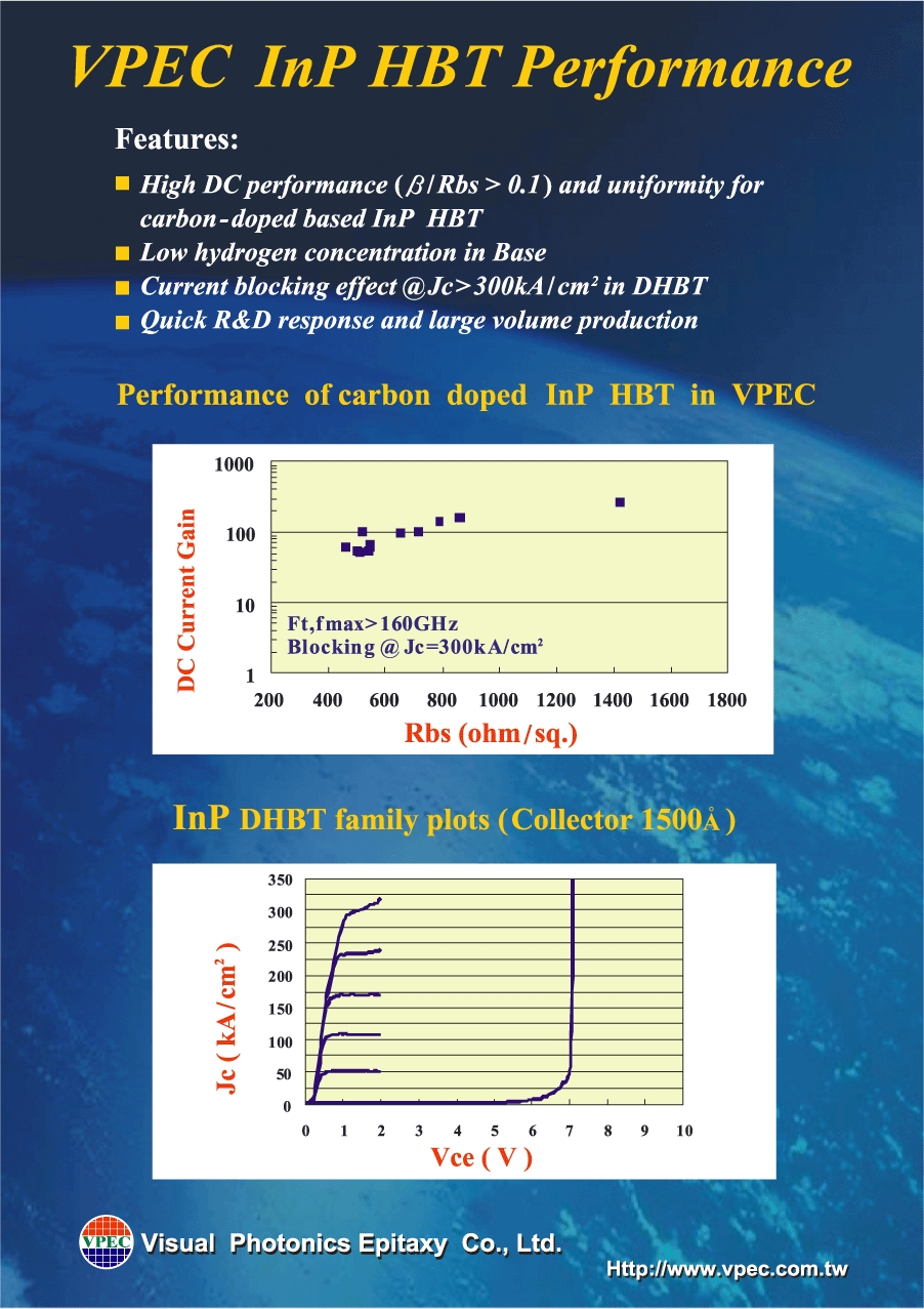
Based on MOCVD epitaxial growth core technology, VPEC has developed state of the art carbon doped base InP HBT epitaxial wafers, with excellent product performance and reliability. VPEC has demonstrated good uniformity of device performance on 4” wafers. VPEC’s InP HBT epitaxial wafers have been qualified by top RF manufacturers worldwide. VPEC’s InP HBT can obtain ft and fmax over 160 GHz. It is an excellent technology for 40Gb/s high speed IC applications in optical fiber communications.