Home > Product Information > Microelectronics epi wafer > High voltage HBT epi wafer
High voltage HBT epi wafer
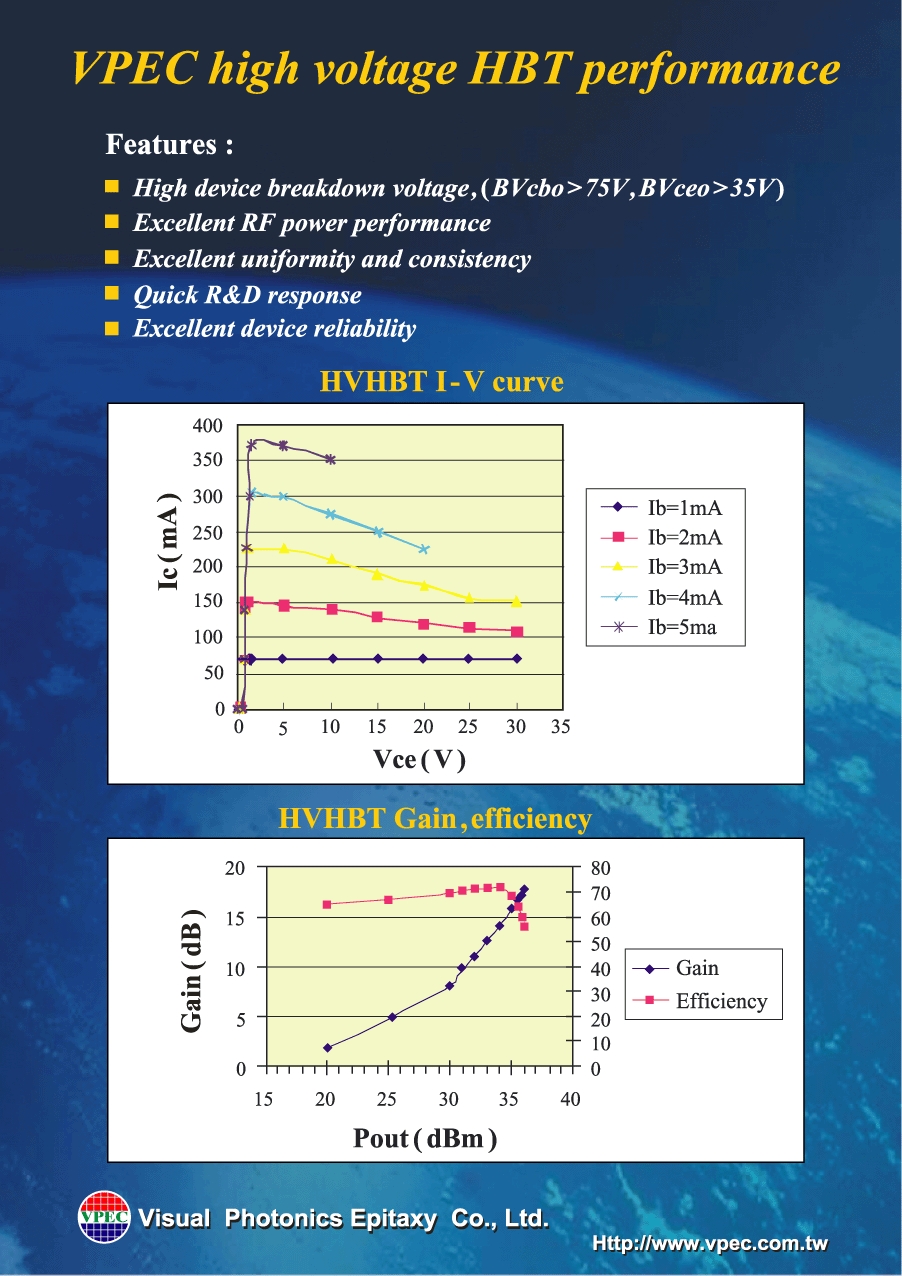
As a result of the superior RF performance of GaAs HBTs, GaAs HBT has become the main stream technology for mobile handset PAs and WLAN. GaAs material has higher band-gap energy and higher breakdown voltage, as compared to Si material devices. This makes GaAs material more suitable than Si for high voltage RF component application. Some applications include RF device testing equipment and base stations for wireless communication infrastructure.
Based on MOCVD epitaxial growth core technology, VPEC has developed high voltage GaAs HBT epitaxial wafers. The base-collector breakdown voltage is over 70 volts and collector-emitter breakdown voltage is over 40 volts. The RF and DC performance of high voltage GaAs HBTs are more suitable for applications in 3G handset base stations and other high voltage RF components than Si. Because of the high quality, high DC and RF performance, reliability, and consistency of VPEC’s high voltage GaAs HBT epitaxial wafers, VPEC’s high voltage GaAs HBT epitaxial wafers has been qualified by top RF manufacturers worldwide when mass production began in Y2006.