Home > Product Information > Microelectronics epi wafer > GaAs HBT epi wafer
GaAs HBT epi wafer
Due to following benefits of GaAs HBT device:
High Linearity
High Speed
High Power Density
Low Phase Noise
Single Power Supply
High Efficiency
GaAs HBT device has wide range applications in wireless communications and optical fiber communications. It is vastly used in power amplifiers (PA), a key component in mobile handsets and wireless local area network (WLAN). From published literature, the PA marketshare for GaAs HBT has ramped up from 10% in Y1995 to 80% in Y2004. GaAs HBT has replaced Silicon (Si) in mainstream PA applications. Furthermore, the rapid expansion of the 3G wireless handset market has increased the demand for GaAs HBT PAs. The multi function requirements of 3G demands more HBT chips per module than 2G or 2.5G handsets.
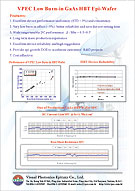
Based on MOCVD epitaxial wafer core technology, VPEC creates state of the art GaAs HBT epi-wafers with excellent product performance and reliability. VPEC’s GaAs HBT epi wafer has obtained qualification from most of the key circuit manufacturers around the world. VPEC controls mass production quality and consistency through its strict quality control system.